Citation
Bogue, R. (2010), "Novel infrared detectors based on black silicon", Sensor Review, Vol. 30 No. 2. https://doi.org/10.1108/sr.2010.08730bab.001
Publisher
:Emerald Group Publishing Limited
Copyright © 2010, Emerald Group Publishing Limited
Novel infrared detectors based on black silicon
Article Type: News From: Sensor Review, Volume 30, Issue 2
Originally developed at Harvard University, black silicon is now being exclusively commercialised by SiOnyx, Inc. and is poised to revolutionise the detection of radiation in the near-IR (NIR) and short-wave IR (SWIR) spectral regions. While these wavelengths can be detected by exotic materials such as germanium, indium gallium arsenide and mercury cadmium telluride, these are expensive and suffer reliability problems. Silicon, on the other hand, is inexpensive and robust and has excellent quantum efficiency in the visible spectrum, making it the leading technology for visible light detection and imaging. Unfortunately, however, the cut-off wavelength and absorption properties of standard crystalline silicon lead to diffuse imagery in the NIR and insensitivity in the SWIR region.
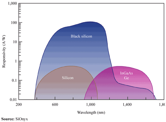
Black silicon (Figure 1) is produced in a CMOS-compatible manufacturing process that uses short-pulse lasers to alter dramatically the properties of silicon. Formed by irradiation with a ultra-fast, femtosecond laser in a sulphur hexafluoride atmosphere, the resulting black silicon comprises a sulphur-doped, nanostructured surface layer that exhibits room temperature photoconductive gain and enhanced IR absorption, yielding responsivities of >100 A/W in the NIR (Figure 2). The manufacturing process is simple, fast and uses standard silicon fabrication materials and conditions.

Potential applications for this technology are numerous and a key use is likely to be in military night vision systems. In addition, the 1,000-1,200 nm region is important for sorting plastic for recycling, solar cell and silicon wafer inspection and non-invasive blood monitoring. Further, the 1,064 nm wavelength is important for applications such as free-space communication and laser detection and ranging. Existing technologies have minimal sensitivity here but black silicon is near its peak performance at 1,064 nm. Devices with sensitivity from 400 to 1,550 nm have been produced and work continues to increase sensitivity to still longer wavelengths.
Rob Bogue