Citation
Bogue, R. (2011), "Spanish company develops unique CMOS-compatible MEMS fabrication process", Assembly Automation, Vol. 31 No. 3. https://doi.org/10.1108/aa.2011.03331caa.002
Publisher
:Emerald Group Publishing Limited
Copyright © 2011, Emerald Group Publishing Limited
Spanish company develops unique CMOS-compatible MEMS fabrication process
Article Type: News From: Assembly Automation, Volume 31, Issue 3
Following four years of R&D, Spanish company Baolab Microsystems has developed a novel technique that allows the fabrication of micro-electromechanical systems (MEMS) devices within the existing metal layers of a CMOS wafer using standard, high volume production methods. Dubbed NanoEMSTM (Nano Embedded Mechanical Systems), this innovative and patented development won the 2010 Elektra European Electronics Industry Awards in the R&D category. Presently with 12 employees, the company was founded in 2003 and has received significant funding from Highgrowth Partners, a Spanish venture capital firm based in Barcelona that specialises in high technology investments.
Traditionally, MEMS devices are constructed on the surface of the silicon during a post-production stage or in a recess in the wafer but this new technique is quicker, simpler and requires fewer process steps. According to the company, this significantly reduces the costs of a MEMS device, by up to two-thirds, or more if several different MEMS are created on the same chip. The process is relatively simple: in the first stage, the MEMS structure is mask-defined within the standard CMOS metal interconnect layers and vias. Patented design methods are used to create the MEMS structures such as inertial masses, suspension springs, capacitive sensing plates, cantilevers and switching contacts. The inter-metal dielectric is then etched away through the pad openings in the passivation layer using vHF (hydrogen fluoride vapour), freeing the MEMS structures. The etching process uses equipment that is already available for volume CMOS production and takes less than an hour. Finally, the holes are sealed and the chip is packaged. As only standard CMOS processes are used, NanoEMS MEMS can be directly integrated with active circuitry for signal conditioning, analogue-digital conversion and digital signal processing. The process is shown in Figure 1, which also illustrates the standard MEMS fabrication technique. Baolab has successfully created MEMS devices using standard 0.18 μm, 8″ CMOS wafers with four or more metal layers and has achieved minimum feature sizes down to 200 nm. This is an order of magnitude smaller than is currently possible with conventional MEMS and Figure 2 shows examples of NanoEMS structures produced by the process.
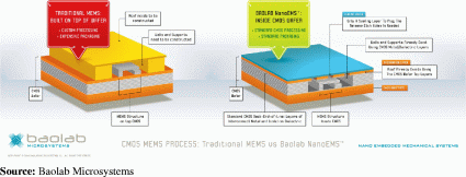

Figure 2 Details of NanoEMS components
Baolab will be producing a range of discrete MEMS devices including RF components and sensors, together with others that combine several functions on a single chip. These are aimed at the rapidly growing but highly competitive and price sensitive mobile phone handset, power amplifier and RF front-end module markets. Sensors will include three-axis digital compasses (magnetometers), three-axis digital accelerometers and a six-DOF tilt-compensated compass, which combines the compass and accelerometer on one chip in a single, standard package. Samples of the first motion sensor products will be available in mid-2011. In mobile phone applications, NanoEMS have several potential uses, ranging from higher performance, lower cost replacements for GaAs FETs for RF switching applications, to tunable, active RF components such as power amplifiers and low-noise amps. Baolab argues that the technology is poised to revolutionise the complex RF front-end section of tomorrow’s mobile phones and tunable components enabled by the integrated switch arrays can dramatically reduce the component count and cost of implementing a 3G/4G mobile phone transceiver.
Contact: Baolab Microsystems, S.L., Institut Politècnic del Campus de Terrassa – Mod. TR25, Cta. Nacional 150, Km 14.5, 08220 Terrassa, Spain. Tel.: +34-93-394-1770, Fax +34-93-736-2137, e-mail: info@baolab.com
Rob Bogue